How to Design 16 Bit Alu Using 4 Bit Alu

Design of ALU :
ALU or Arithmetic Logical Unit is a digital circuit to do arithmetic operations like addition, subtraction,division, multiplication and logical oparations like and, or, xor, nand, nor etc. A simple block diagram of a 4 bit ALU for operations and,or,xor and Add is shown here :
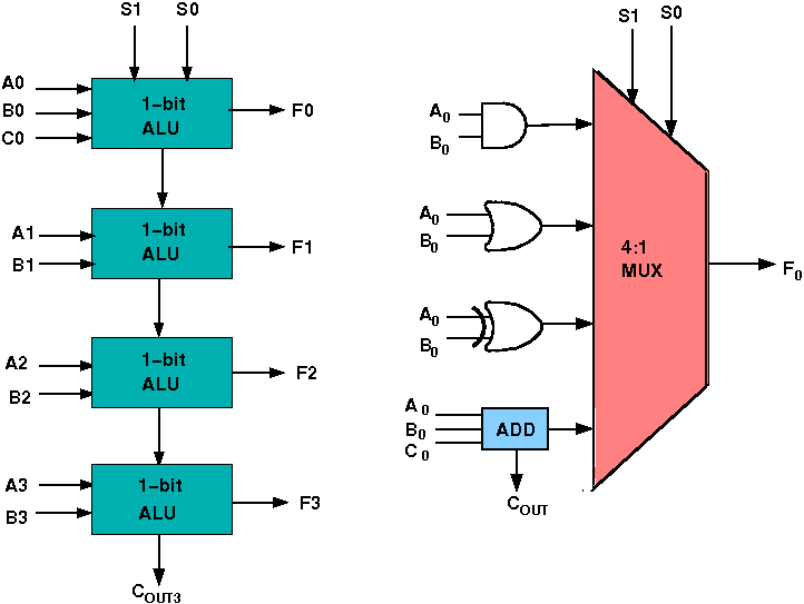
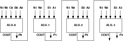
The 4-bit ALU block is combined using 4 1-bit ALU block
Design Issues :
The circuit functionality of a 1 bit ALU is shown here, depending upon the control signal S1 and S0 the circuit operates as follows:
for Control signal S1 = 0 , S0 = 0, the output is A And B,
for Control signal S1 = 0 , S0 = 1, the output is A Or B,
for Control signal S1 = 1 , S0 = 0, the output is A Xor B,
for Control signal S1 = 1 , S0 = 1, the output is A Add B.
The truth table for 16-bit ALU with capabilities similar to 74181 is shown here:
| Mode Select | Fn for active HIGH operands | ||||
|---|---|---|---|---|---|
| Inputs | Logic | Arithmetic (note 2) | |||
| S3 | S2 | S1 | S0 | (M = H) | (M = L) (Cn=L) |
| L | L | L | L | A' | A |
| L | L | L | H | A'+B' | A+B |
| L | L | H | L | A'B | A+B' |
| L | L | H | H | Logic 0 | minus 1 |
| L | H | L | L | (AB)' | A plus AB' |
| L | H | L | H | B' | (A + B) plus AB' |
| L | H | H | L | A ⊕ B | A minus B minus 1 |
| L | H | H | H | AB' | AB minus 1 |
| H | L | L | L | A'+B | A plus AB |
| H | L | L | H | (A ⊕ B)' | A plus B |
| H | L | H | L | B | (A + B') plus AB |
| H | L | H | H | AB | AB minus 1 |
| H | H | L | L | Logic 1 | A plus A (Note 1) |
| H | H | L | H | A+B' | (A + B) plus A |
| H | H | H | L | A+B | (A + B') plus A |
| H | H | H | H | A | A minus 1 |
The L denotes the logic low and H denotes logic high.
Design of ALU :
Basic stage
Multiple choice questions:
- Maximum number of inputs to a data selector having 3 control pins
- How many 3 to 8 line decoders are required for a 1-of-32 decoder?
- What is the minimum number of two input NAND gates used to perform the function of two input OR gate ?
- A controlled inverter gives the 1's complement of the input
- The number of canonical expressions that can be developed over a 3-valued boolean algebra is
- A switching function is symmetric with respect to a set of literals if and only if the function remains unchanged after
3
8
4
9
8
1
4
2
2
4
3
5
True
False
16
32
64
8
Any permutation of the literals
All the literals are changed in clockwise order
Two of these literals are interchanged
All the literals are changed in anticlockwise order
Subjective questions:
- What does the selector inputs to an arithmetic logic unit (ALU) determine?
- How to design 16-bit ALU using 4-bit ALU?
Advanced stage
Multiple choice questions:
- Both the ALU and control unit of CPU employ special purpose storage which is called
- The number of levels in the design of a 64 X 1 mux using 4 X 1 mux
- On which factor the number of functions realized by a decoder depends?
- One mux can realize one function at a time and the functional dependency can be preseved in multilevel realizations
Registers
Buffers
Decoders
Multiplexers
4
5
3
2
Number of gates
Fanout capacity
Both
None of these
True
False
In 2's complement overflow
Can not occur when a positive value is added to a negative value
Is flagged whenever there is carry from sign bit addition
Is flagged when the carry from sign bit and previous bit matches
None of these
Subjective questions:
- Desig an ALU with one select variable s and two data inputs A and B. when s=0, the circuit performs addition operation F=A+B. when s=1, the circuit performs increment operation F=A+1
- Describe with a schematic diagram, how the ALU is connected to the processor registers through common bus.
Design of ALU :
Procedure to perform the experiment:Design of 4 bit ALU
- Start the simulator as directed.This simulator supports 5-valued logic.
- To design the circuit we need 4 1-bit ALU, 11 Bit switch (to give input,which will toggle its value with a double click), 5 Bit displays (for seeing output), wires.
- The pin configuration of a component is shown whenever the mouse is hovered on any canned component of the palette. Pin numbering starts from 1 and from the bottom left corner (indicating with the circle) and increases anticlockwise.
- For 1-bit ALU input A0 is in pin-9,B0 is in pin-10, C0 is in pin-11 (this is input carry), for selection of operation, S0 is in pin-12, S1 is in pin-13, output F is in pin-8 and output carry is pin-7
- Click on the 1-bit ALU component (in the Other Component drawer in the pallet) and then click on the position of the editor window where you want to add the component (no drag and drop, simple click will serve the purpose), likewise add 3 more 1-bit ALU (from the Other Component drawer in the pallet), 11 Bit switches and 5 Bit Displays (from Display and Input drawer of the pallet,if it is not seen scroll down in the drawer), 3 digital display and 1 bit Displays (from Display and Input drawer of the pallet,if it is not seen scroll down in the drawer)
- To connect any two components select the Connection menu of Palette, and then click on the Source terminal and click on the target terminal. According to the circuit diagram connect all the components. Connect the Bit switches with the inputs and Bit displays component with the outputs. After the connection is over click the selection tool in the pallete.
- See the output, in the screenshot diagram we have given the value of S1 S0=11 which will perform add operation and two number input as A0 A1 A2 A3=0010 and B0 B1 B2 B3=0100 so get output F0 F1 F2 F3=0110 as sum and 0 as carry which is indeed an add operation.you can also use many other combination of different values and check the result. The operations are implemented using the truth table for 4 bit ALU given in the theory.
Circuit Diagram
Components :
To build any 4 bit ALU, we need :
- AND gate, OR gate, XOR gate
- Full Adder,
- 4-to-1 MUX<
- Wires to connect.
In case of counters the number of flip-flops depends on the number of different states in the counter.
Objective of 4 bit arithmetic logic unit (with AND, OR, XOR, ADD operation):
- Understanding behaviour of arithmetic logic unit from working module and the module designed by the student as part of the experiment
- Designing an arithmetic logic unit for given parameter
Examining behaviour of arithmetic logic unit for the working module and module designed by the student as part of the experiment (refer to the circuit diagram):
Loading data in the arithmetic logic unit (refer to procedure tab for further detail and experiment manual for pin numbers):
- load the two input numbers as:
- A(A3 A2 A1 A0): A3=1, A2=1, A1=0, A0=0
- B(B3 B2 B1 B0): B3=1, B2=0, B1=0, B0=1
- carry in(C0)=0
examining the AND behaviour:
- load data in select input as:
- S1=0, S0=0 `
- check output:
- F3=1, F2=0, F1=0, F0=0
- cout=0 `
examining the OR behaviour:
- load data in select input as:
- S1=0, S0=1 `
- check output:
- F3=1, F2=1, F1=0, F0=1
- cout=0 `
examining the XOR behaviour:
- load data in select input as:
- S1=1, S0=0 `
- check output:
- F3=0, F2=1, F1=0, F0=1
- cout=0 `
examining the ADD behaviour:
- load data in select input as:
- S1=1, S0=1 `
- check output:
- F3=0, F2=1, F1=0, F0=1
- cout=1 `
Recommended learning activities for the experiment: Leaning activities are designed in two stages, a basic stage and an advanced stage. Accomplishment of each stage can be self-evaluated through the given set of quiz questions consisting of multiple type and subjective type questions. In the basic stage, it is recommended to perform the experiment firstly, on the given encapsulated working module, secondly, on the module designed by the student, having gone through the theory, objective and procuder. By performing the experiment on the working module, students can only observe the input-output behavior. Where as, performing experiments on the designed module, students can do circuit analysis, error analysis in addition with the input-output behavior. It is recommended to perform the experiments following the given guideline to check behavior and test plans along with their own circuit analysis. Then students are recommended to move on to the advanced stage. The advanced stage includes the accomplishment of the given assignments which will provide deeper understanding of the topic with innovative circuit design experience. At any time, students can mature their knowledge base by further reading the references provided for the experiment.
- if value is UNKNOWN, wire color= maroon
- if value is TRUE, wire color= blue
- if value is FALSE, wire color= black
- if value is HI IMPEDENCE, wire color= green
- if value is INVALID, wire color= orange
likewise the 16 bit arithmetic logic unit can be designed and tested
- by cascading 4 bit ALUs only the carry will propagate to the next level for ADD operation
Test plan :
- Set inputs 0101 and 0011 and check output for all possible select input combinations.
- Set any two 16-bit number and check output for all possible select input combinations.
Use Display units for checking output. Try to use minimum number of components to build. The pin configuration of the canned components are shown when mouse hovered over a component.
Assignment Statements :
- Design a 4 bit ALU comprising only the AND, OR, XOR and Add operations.
- Design a 16-bit ALU with capabilities similar to 74181
Design of ALU :
General guideline to use the simulator for performing the experiment:
- Start the simulator as directed. For more detail please refer to the manual for using the simulator
- The simulator supports 5-valued logic
- To add the logic components to the editor or canvas (where you build the circuit) select any component and click on the position of the canvas where you want to add the component
- The pin configuration is shown when you select the component and press the 'show pinconfig' button in the left toolbar or whenever the mouse is hovered on any canned component of palette
- To connect any two components select the connection tool of palette, and then click on the source terminal and then click on the the target terminal
- To move any component select the component using the selection tool and drag the component to the desired position
- To give a toggle input to the circuit, use 'Bit Switch' which will toggle its value with a double click
- Use 'Bit Display' component to see any single bit value. 'Digital Display' will show the output in digital format
- undo/redo, delete, zoom in/zoom out, and other functionalities have been given in the top toolbar for ease of circuit building
- Use start/stop clock pulse to start or stop the clock input of the circuit. Clock period can be set from the given 'set clock' button in the left toolbar
- Use 'plot graph' button to see input-output wave forms
- Users can save their circuits with .logic extension and reuse them
- After building the circuit press the simulate button in the top toolbar to get the output
- If the circuit contains a clock pulse input, then the 'start clock' button will start the simulation of the whole circuit. Then there is no need to again press the 'simulate' button
- If you are using linux platform then click on 'Linux(32 bit)' or if you are using then click on 'Windows(32 bit)'
Linux(32 bit)
Windows(32 bit)
Circuit diagram of 4 bit ALU:
Screenshot of Design of 4 bit ALU:

Back
Circuit diagram of 4 bit ALU:
Screenshot of Design of 4 bit ALU:
Back
Guideline to perform the experiment:Design of 4 bit ALU
- Start the simulator as directed.
- To design the circuit we need 4 1-bit ALU, 11 Bit switch (to give input,which will toggle its value with a double click), 5 Bit displays (for seeing output), wires.
- The pin configuration of a component is shown whenever the mouse is hovered on any canned component of the palette. Pin numbering starts from 1 and from the bottom left corner (indicated with the circle) and increases anticlockwise.
- For 1-bit ALU input A0 is in pin-9,B0 is in pin-10, C0 is in pin-11 (this is input carry), for selection of operation, S0 is in pin-12, S1 is in pin-13, output F is in pin-8 and output carry is pin-7
- Click on the 1-bit ALU component (in the Other Component drawer in the pallet) and then click on the position of the editor window where you want to add the component (no drag and drop, simple click will serve the purpose), likewise add 3 more 1-bit ALU (from the Other Component drawer in the pallet), 11 bit switches and 5 bit displays (from Display and Input drawer of the pallet,if it is not seen scroll down in the drawer), 3 digital display and 1 bit displays (from Display and Input drawer of the pallet,if it is not seen scroll down in the drawer)
- To connect any two components select the Connection menu of Palette, and then click on the Source terminal and click on the target terminal. According to the circuit diagram connect all the components. Connect the Bit switches with the inputs and Bit displays component with the outputs. After the connection is over click the selection tool in the pallete.
- See the output, in the screenshot diagram we have given the value of S1 S0=11 which will perform add operation and two number input as A0 A1 A2 A3=0010 and B0 B1 B2 B3=0100 so get output F0 F1 F2 F3=0110 as sum and 0 as carry which is indeed an add operation.you can also use many other combination of different values and check the result. The operations are implemented using the truth table for 4 bit ALU given in the theory.
Circuit Diagram
Click here to download the older version of simulator
Click here to download the new version of simulator
OR
Launch the older version of Simulator
Launch the new version of Simulator
Once the simulator is downloaded, open the command prompt, then go to the directory where you have saved it using cd command and then give the following command to run the simulator:
java -jar coaSimulator.jar
Guideline to perform the experiment:Design of 4 bit ALU
- Start the simulator as directed.
- To design the circuit we need 4 1-bit ALU, 11 Bit switch (to give input,which will toggle its value with a double click), 5 Bit displays (for seeing output), wires.
- The pin configuration of a component is shown whenever the mouse is hovered on any canned component of the palette or press the 'show pinconfig' button. Pin numbering starts from 1 and from the bottom left corner (indicated with the circle) and increases anticlockwise.
- For 1-bit ALU input A0 is in pin-9,B0 is in pin-10, C0 is in pin-11 (this is input carry), for selection of operation, S0 is in pin-12, S1 is in pin-13, output F is in pin-8 and output carry is pin-7
- Click on the 1-bit ALU component(in the Other Component drawer in the pallet) and then click on the position of the editor window where you want to add the component (no drag and drop, simple click will serve the purpose), likewise add 3 more 1-bit ALU (from the Other Component drawer in the pallet), 11 Bit switches and 5 bit displays (from Display and Input drawer of the pallet,if it is not seen scroll down in the drawer), 3 digital display and 1 bit Displays (from Display and Input drawer of the pallet,if it is not seen scroll down in the drawer)
- To connect any two components select the Connection menu of Palette, and then click on the Source terminal and click on the target terminal. According to the circuit diagram connect all the components. Connect the Bit switches with the inputs and Bit displays component with the outputs. After the connection is over click the selection tool in the pallete.
- See the output, in the screenshot diagram we have given the value of S1 S0=11 which will perform add operation and two number input as A0 A1 A2 A3=0010 and B0 B1 B2 B3=0100 so get output F0 F1 F2 F3=0110 as sum and 0 as carry which is indeed an add operation.you can also use many other combination of different values and check the result. The operations are implemented using the truth table for 4 bit ALU given in the theory.
Circuit Diagram
Click here to download the older version of simulator
Click here to download the new version of simulator
OR
Launch the older version of Simulator
Launch the new version of Simulator
Once the simulator is downloaded, open the command prompt, then go to the directory where you have saved it using cd command and then give the following command to run the simulator:
java -jar Simulator.jar
Design of ALU :
References :
Books:
- Digital Logic and Computer Design - M. Morris Mano. Pearson Education - Prentice Hall.
- Computer Architecture and Organization - John P. Hayes
- Digital Principles Foundation of Circuit Design and Application - Arun Kumar Singh. New Age Publishers.
- The Art of Electronics - Paul Horowitz and Winfield Hill (1989). Cambridge University Press
- Modern Dictionary of Electronics - Rudolf F. Graf (1999). Newnes
Web Sites:
- http://library.thinkquest.org/25111/alu.shtml
- http://en.wikipedia.org/wiki/Arithmetic_logic_unit
- NPTEL (e-learning courses from IITs and IISC)
Virtual Lab is an initiative of Ministry of Human Resource and Development(MHRD) under National Mission of Education through ICT to provide an interactive environment over the internet for creating and conducting different laboratory experiments by sharing the costly equipments and the resources.
For more information about the Virtual Lab,please visit http://www.vlab.co.in/
Developers of Logic Design and Computer Organization Virtual Lab
- Dr. Chittaranjan Mandal Professor, Computer Science & Engineering
- Gargi Roy Senior Project Assistant
- Devleena Ghosh
Professor, Information Technology
IIT Kharagpur
Target Audience:
Under graduate students.
Courses Aligned With:
Digital Logic and Computer organization.
Pre-requisite Softwares:
- 32 bit java runtime environment and java 1.6 or above
- Recommended browser: mozilla firefox, google chrome
Objectives:
The Objective is to Expose the students to the various key aspects of Computer Organisation by enabling them to perform FPGA based prototyping of experiments with support of a virtual environment. The primary need for virtualisation here is multifold.
- Digital Logic and Computer Organisation are core courses in most of the Undergraduate Curricula of the entire Electrical Sciences Discipline(Computer Science / Engg., Electronics, Electrical) etc.
- Many colleges/institutes cannot procure sufficient number of FPGA boards for their students.
- Even when such FPGA boards are available, making them available round the clock is difficult.
- Expert help is required to effectively use these FPGA boards and such help can be easily channeled through a virtual environment.
- Helps to standardize the set of Experiments to a large extent.
Feedback:
To give your feedback please visit the following link-
Sponsered by MHRD (NME-ICT) .
Contact Information:
Mailing Address and Contact Information:
Department of Computer Science & Engineering, IIT Kharagpur
Office : +91-3222-2882255
Postal Address:
Indian Institute of Technology Kharagpur, Kharagpur - 721302, INDIA Telephone Number +91-3222-255221 | FAX : +91-3222-255303
Tutorial on UI for lab:
Introduction:
- The simulator contains a pallete on the right hand side. This pallete contains all the components and tools . Tools are used to act up on the components. Different tools:
- Selection tool- used for selecting components
- Marquee tool- used for selecting many components at a time by draggiung the mouse in the design area(editor).
- Connection tool- used for connecting components
- Components have been catagorized according to their functionality and put into different drawers in the pallete. The area under every drawer is scrallable, if you are unable to see all the components in a particular drawer just click on the area and scroll. Different drawers:
- Circuits- contains 8 and 16 terminal circuits and flow container which can hold other circuit components.
- Logic gates- contains all kinds of basic logic gates.
- Display and inputs- contains all kinds of component needed to give input to the circuit and displaying outputs of the circuit.
- Adders- contains different types of adder circuits.
- Sequential ckt- contains basic flipflops for designing sequential circuits.
- Other Components- contains different kinds of components like decoders, multiplexers, arithmetic logic units(ALU), memory elements(RAM cell) required to design combinational circuits.
- To add the components to the editor select any component(first click on the selection tool then click on the desired compoent) then finally click on the position of the editor window where you want to add the component.
- The pin configuration of a component is shown whenever the mouse is hovered on any canned component of the palette. Pin numbering starts from 1 and from the bottom left corner(indicating with the circle) and increases anticlockwise.
- To connect any two components select the Connection tool in the palette, and then click on the Source terminal and click on the target terminal(no drag and drop, simple click will serve the purpose). After the connection is over click the selection tool in the pallete.
- To move any components select the Selection Mode and drag the component after selecting it.
- If needed select any component in the editor while designing your circuit and use Undo, Redo, Delete,Zoom in, Zoom out buttons to get corresponding functionalities. Open and Save options are under development.
- As the automated clock is under development and the simulator is under modification for sequencial circuits, for the time being please use individual clock(Bit switch which toggle its value with a double click) for each flipflop.
- The simulator is currently under modification for sequential circuits, now it is working properly for combinational circuits but may not give proper output for sequential circuits.
Description of Components:
General components:
- Digital display: it can be used to give input and as well as to see the output in the decimal format, its right most terminal is the LSB(least significant bit) and the left most terminal is the MSB(most significant bit), in the editor after selecting a particular digital display you can use 'Increment LED' and 'Decrement LED' buttons in the top left corner of the simulator to increment and decrement its value respectively.
- Bit display: it displays a single bit value.
- V+: it gives 1 as input.
- Ground: it gives 0 as input.
- Bit switch: it gives 1/0 input, it toggels its value with a double click.
Specific components:
Specific components:
Pin numbering starts from 1 and from the bottom left corner(indicating with the circle) and increases anticlockwise. Pin configurations of all the components-
- Half adder: i/p: 5,8o/p: sum=4, carry=1
- Full adder: i/p: 5,6,8o/p: sum=4, carry=1
- RCA 4 bit: (4 bit ripple carry adder) i/p: A0=13,A1=14,A2=15,A3=16; B0=17,B1=18,B2=19,B3=20; C0=21o/p: S0=12,S1=11,S2=10,S3=9,Cout=8
- Wallace tree adder: (adds 3 4-bit numbers) i/p: A0=13,A1=14,A2=15,A3=16; B0=17,B1=18,B2=19,B3=20; C0=21,C1=22,C2=23,C3=24o/p: S0=12,S1=11,S2=10,S3=9,Cout=8
- RS flipflop: i/p: R=5, S=8, Clk=7o/p: Q=4, Q'=1
- D flipflop: i/p: D=5, Clk=8o/p: Q=4, Q'=1
- T flipflop: i/p: T=8, Clk=7o/p: Q=4, Q'=1
- JK flipflop: i/p: J=5, K=8, Clk=7o/p: Q=4, Q'=1
- 2:4 Decoder: i/p: A0=5,A1=7o/p: D0=4,D1=3,D2=2,d3=1
- 2:4 Decoder with enable: i/p: A=6,B=5,Enable=8o/p: D0=4,D1=3,D2=2,d3=1
- 4:1 Mux: i/p: I0=9,I1=10,I2=11,I3=12,S0=13,S1=14o/p: F=8
- Combinational Multiplier: i/p: multiplicand: A0=13,A1=14,A2=15,A3=16Multiplier: B0=9,B1=10,B2=11,B3=12o/p: S0=8,S1=7,S2=6,S3=5,S4=4,S5=3,S6=2,S7=1
- ALU 1 bit: i/p: A0=9, B0=10, C0=21 S0=12,S1=13o/p: F=8, Cout=7
- 4 bit ALU: i/p: A0=13,A1=14,A2=15,A3=16; B0=17,B1=18,B2=19,B3=20; C0=21;S0=22,S1=23o/p: F0=12,F1=11,F2=10,F3=9,Cout=8
- 16 bit ALU: i/p: A1=13,A2=15; B1=14,B2=16; Cin=9,S0=12,S1=11,S2=10o/p: Cout=6,F2=7,F1=8
- RAM Cell: i/p=5,select=8,R/W'=6,o/p=4, R/W'=1 for read operation,R/W'=0 for write operation
- IC Memory: R/W'=16Memory Enable=15,Address i/p=14,13Data i/p=12,11,10Data o/p=6,7,8R/W'=1 for read operation,R/W'=0 for write operation
- Direct Mapped Cache:
- pin-32= S(selects whether user wants to perform cache write or cache mapping)
- pin-31= R/W'A(selects whether user wants to input the address or cache mapping)
- pin-30=A3, pin-29=A2, pin-28=A1, pin-27=A0 (thise 4 pins are used to give address input). A3 is the most significant bit and A0 is the least significant bit. A3 and A2 will be compared with the tag. A1 and A0 will select the corrsponding set.
- pin-26= R/W'D(selects whether user wants to input in the set of cache or cache mapping)
- pin-25= M1, pin-24=M0 (M1 is the most significant bit and M0 is the least significant bit). thiese two bits are used for cache writhe purpose, it selects the particular set of which user wants to give inputs to the valid bit, tag bits and data bits.
- pin-23= Den(this is an enable input which has to set for any write purpose in the cache).
- pin-21= valid bit
- pin-20= T1, pin-19=T0 (T1 is the most significant bit and T0 is the least significant bit). These are tag bits.
- pin-18= D1, pin-17=D0 (D1 is the most significant bit and D0 is the least significant bit). These are data bits.
- pin-14= Hit/Miss bit(if it gives 1 then hit otherwise miss)
- pin-15= F1, pin-16=F0 (F1 is the most significant bit and F0 is the least significant bit). These are output data bits and will be given only when there is a hit.
- Essential pin configurations for writing in cache: S=1, R/W'A=0, R/W'D=0, Den= 1
- Essential pin configurations for cache mapping: S=0, R/W'A=1, R/W'D=1, Den= 0
Hide specific components
Testing process:
- To test your circuit give some input(through Digital display or Bit switch or V+ or Ground), if you use the Digital display or Bit switch you can then give different input to you circuit through incrementing/decrementing the Digital display or double clicking the Bit switch, the other two gives constant inputs.
- to see the output, connect Digital display or Bit display to the output terminals of your circuit.
Go to the Top
Frequently Asked Questions:
What is virtual lab?
The Virtual Laboratory is an interactive environment for creating and conducting simulated experiments: a playground for experimentation. It consists of domain dependent simulation programs, experimental units called objects that encompass data files, tools that operate on these objects.
What are the advantages of virtual lab?
Virtual Logic Design and Computer Organisation lab enables students to perform FPGA based prototyping of experiments with support of a virtual environment. The primary need for virtualisation here is multifold.
- Digital Logic and Computer Organisation are core courses in most of the Undergraduate Curricula of the entire Electrical Sciences Discipline ( Computer Science / Engg., Electronics, Electrical ] etc.
- Many colleges/institutes cannot procure sufficient number of FPGA boards for their students.
- Even when such FPGA boards are available, making them available round the clock is difficult.
- Expert help is required to effectively use these FPGA boards and such help can be easily channeled through a virtual environment.
- Helps to standardize the set of Experiments to a large extent.
What is eclipse platform?
Eclipse is a Java-based, extensible open source development platform. By itself, it is simply a framework and a set of services for building a development environment from plug-in components. Eclipse comes with a standard set of plug-ins, including the Java Development Tools (JDT).
Which framework is used to develop the application?
We have used the eclipse gef framework. The Graphical Editing Framework (GEF) allows developers to take an existing application model and quickly create a rich graphical editor.
What is platform independent application?
Applications that run under particular operating systems and/or particular hardwares are called platform dependent application whereas platform independent applications can run in any operating environment.
What are the experiments which can be performed by the Virtual Logic Design and Computer Organization lab?
The experiments that will be supported by this lab are given below:
- Design of a ripple carry adder
- Design of a carry-look-ahead adder
- Design of registers and counters
- Design of a wallace tree adder
- Design of combinational multipliers
- Design of a Booth's multiplier
- Design of an ALU
- Design of memory units
- Design of direct mapped cache
- Design of associative cache
- Design of combinational dividers
- CPU design
How to Design 16 Bit Alu Using 4 Bit Alu
Source: https://cse.iitkgp.ac.in/~chitta/coldvl/alu.html
0 Response to "How to Design 16 Bit Alu Using 4 Bit Alu"
Post a Comment